
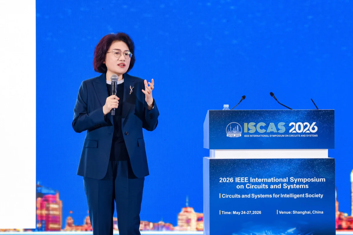
SHANGHAI – In a defiant move against persistent U.S. export restrictions, Chinese tech behemoth Huawei announced on Monday a groundbreaking new engineering approach to advanced semiconductor development, dubbed "LogicFolding." The revelation, presented by Tingbo He, president of Huawei’s semiconductor business, at a high-profile industry conference in Shanghai on May 25, 2026, signals a significant escalation in China’s push for technological self-sufficiency and poses a direct challenge to the global chip industry’s established paradigms. This strategic unveiling comes as American chip giant Nvidia grapples with the fallout of U.S. sanctions, struggling to sell its most advanced artificial intelligence (AI) chips in the lucrative Chinese market, effectively ceding significant ground to Huawei.
Huawei’s new methodology, LogicFolding, is slated to underpin its next generation of Kirin smartphone chips, with an anticipated launch this fall. This innovation is more than just a technical upgrade; it represents a strategic pivot designed to circumvent the chokehold of U.S. sanctions, which have severely hampered Huawei’s access to cutting-edge chip manufacturing tools and intellectual property from Western suppliers. The company’s announcement reverberates across the global technology landscape, particularly in the context of intensifying geopolitical competition and the ongoing U.S.-China tech rivalry. The timing is particularly poignant, following recent statements by Nvidia CEO Jensen Huang, who acknowledged that his company had "conceded" the Chinese AI chip market to Huawei, highlighting the effectiveness of China’s domestic acceleration efforts.
A Decade of Defiance: Huawei’s Sanctions Journey
The backdrop to Huawei’s latest announcement is a tumultuous period marked by stringent U.S. sanctions, which began in earnest in 2019. Initially placed on the Entity List by the U.S. Commerce Department, Huawei found its access to critical American technology, software, and components severely restricted. The rationale behind these measures, as articulated by Washington, centered on national security concerns, alleging that Huawei’s equipment could be used by the Chinese government for espionage. Huawei consistently denied these accusations, but the sanctions progressively tightened, culminating in rules that barred any company using U.S. technology from supplying chips to Huawei without a special license. This move effectively cut Huawei off from its primary chip suppliers, including TSMC, the world’s leading contract chip manufacturer.
For years, these restrictions crippled Huawei’s smartphone business, which once vied for the top spot globally. The inability to procure advanced 5G-capable chips forced the company to release 4G-only devices, ceding significant market share to competitors like Apple and Samsung. However, Huawei embarked on an ambitious, state-backed drive to foster domestic alternatives. This arduous journey began yielding tangible results in late 2023 with the surprise launch of its Mate 60 smartphone series. Equipped with a domestically produced, advanced 5G-capable chip – widely believed to be manufactured by China’s Semiconductor Manufacturing International Corporation (SMIC) using an older but highly optimized 7-nanometer process – the Mate 60 Pro became a symbol of national technological resilience. The device’s unexpected success spurred a resurgence for Huawei in the Chinese market, directly impacting Apple’s sales and market share in the world’s second-largest consumer economy. This comeback demonstrated China’s growing capability to overcome foreign technological blockades, albeit at immense cost and effort.
LogicFolding: A New Frontier in Chip Architecture
At the heart of Huawei’s latest declaration is LogicFolding, an engineering approach that Tingbo He described as a paradigm shift in semiconductor manufacturing. While specific technical details remain under wraps, He indicated that this architecture expands the traditional two-dimensional chip layout from one layer to two, dramatically enhancing power efficiency and transistor density. This multi-layered design allows for significantly more interaction points between transistors, theoretically enabling more complex computations within a smaller footprint and with reduced energy consumption. This approach echoes broader industry trends towards 3D stacking and advanced packaging, but Huawei positions LogicFolding as a distinct, proprietary methodology that could circumvent traditional lithography challenges.
Huawei boldly claims that by 2031, its new chip technology could deliver capabilities equivalent to a 1.4-nanometer process technology. This assertion is particularly audacious given the current state of global chip manufacturing, where industry leader TSMC has only recently commenced volume production of 2-nanometer chips, with 3-nanometer processes already in widespread use for high-end devices. Nanometer process nodes refer to the minimum feature size on a chip, with smaller nodes generally translating to higher transistor density, faster processing speeds, and improved power efficiency.
However, industry experts, including Paul Triolo, head of technology, Asia and Americas, at DGA Group, express a degree of skepticism regarding Huawei’s 1.4-nanometer claim. "A stacked/folded design can produce effective density gains, but it does not mean Huawei has solved the full process, yield, power, thermal, and device-performance problems associated with true 1.4 nm-class manufacturing," Triolo commented. He highlighted that while architectural innovations can enhance performance and efficiency, they do not inherently resolve the immense challenges of manufacturing at such minuscule scales, including maintaining high yield rates, managing heat dissipation, and ensuring long-term device reliability. The leap from laboratory concept to mass production at competitive costs remains a monumental hurdle.
The "Law of Tau" and the Post-Moore’s Law Era
Beyond the engineering specifics of LogicFolding, Huawei is also seeking to establish a new theoretical framework for its semiconductor research, introducing what it calls the "Law of Tau," or "τ scaling." This initiative aims for greater academic recognition and positions Huawei as a thought leader addressing the fundamental challenges facing the semiconductor industry in the post-Moore’s Law era. For decades, semiconductor development has been guided by Moore’s Law, an empirical observation by Intel co-founder Gordon Moore in 1965 that the number of transistors on a microchip would double approximately every two years, leading to exponential increases in computing power and corresponding reductions in cost.
However, the physical limits of silicon-based lithography are increasingly being reached, making it exponentially more difficult and expensive to shrink transistors further. Even industry luminaries like Nvidia’s Jensen Huang have publicly stated that Moore’s Law is "no longer applicable" to future chip development. Huawei’s "Law of Tau" emerges in this context, attempting to provide a new guiding principle. Paul Triolo described it as "more a systems-level optimization doctrine: shorten wires, stack logic, improve memory semantics, and co-design chips, packages, software, and clusters." This perspective suggests that future performance gains will not solely come from shrinking transistors but from holistic improvements across chip architecture, packaging, software optimization, and system-level integration. Tingbo He, who also serves as a director of Huawei’s scientist committee, elaborated on this during her presentation at the Institute of Electrical and Electronics Engineers’ International Symposium on Circuits and Systems, noting that while the potential is immense, Huawei is only at the beginning of what she acknowledges will be a decade-long development path for the new technology. The challenges of heat management and manufacturing at scale remain formidable, underscoring the long road ahead for this ambitious undertaking.
Market Repercussions and Geopolitical Implications
Huawei’s bold announcement has immediate and profound implications for the global technology market and the geopolitical landscape. For Nvidia, the implications are particularly acute. U.S. export restrictions have, in recent years, prevented Nvidia from selling its most advanced AI accelerators, such as the A100 and H100, to China. Subsequent attempts to offer "watered-down" versions, like the H800 and L20, specifically designed to comply with U.S. regulations, have met with limited success. Chinese customers, including major cloud providers and tech companies, have shown a clear preference for domestically developed alternatives or are investing heavily in their own AI chip development. George Chen, partner and co-chair of digital practice at The Asia Group, succinctly summarized the situation: "For Nvidia, this means the window to sell advanced chips such as the H200 into China is narrowing." He added, "This trajectory will likely heighten concerns in Washington, where Huawei remains emblematic of U.S. export restrictions."
The competitive landscape for smartphones in China is also experiencing a significant shift. Huawei’s Mate 60 resurgence, fueled by its domestically produced 5G chip, has already eaten into Apple’s market share. If LogicFolding delivers on its promises, Huawei could further strengthen its position, potentially releasing devices that offer performance competitive with, or even superior to, Western counterparts in certain metrics. This would mark a dramatic turnaround for a company many had written off in the premium smartphone segment.
Beyond smartphones, the implications extend to critical sectors like artificial intelligence, cloud computing, and advanced computing infrastructure. China’s national strategy prioritizes self-reliance in key technologies, and breakthroughs from companies like Huawei are seen as vital steps toward reducing dependence on foreign suppliers. The Chinese government has poured billions into its domestic semiconductor industry, fostering companies like SMIC and YMTC, to build a robust indigenous supply chain. Huawei’s LogicFolding announcement, therefore, is not merely a corporate achievement but a significant milestone in China’s broader strategic technological independence.
From a U.S. policy perspective, Huawei’s advancements will undoubtedly trigger renewed scrutiny and potentially new policy responses. Washington’s stated goal has been to slow China’s technological progress, particularly in areas with dual-use potential (civilian and military applications). Huawei’s ability to innovate under sanctions complicates this strategy, suggesting that while sanctions impose costs, they also act as a powerful catalyst for indigenous innovation. U.S. officials are likely to closely monitor the actual performance and manufacturability of Huawei’s LogicFolding chips, evaluating whether the claims translate into commercially viable, high-volume production. The debate within Washington will intensify, weighing the effectiveness of current restrictions against the unintended consequence of accelerating China’s self-sufficiency.
Industry observers also note that while Huawei’s claims are ambitious, the company has a strong track record of significant R&D investment and engineering prowess. However, the path from advanced architectural design to high-volume, cost-effective manufacturing is fraught with challenges, particularly without access to the most advanced extreme ultraviolet (EUV) lithography machines, which are crucial for producing sub-7nm chips and are largely controlled by Dutch firm ASML under U.S. pressure. Huawei’s approach, therefore, likely involves optimizing existing manufacturing processes and leveraging innovative design to compensate for limitations in lithography.
In conclusion, Huawei’s introduction of LogicFolding and the "Law of Tau" represents a pivotal moment in the global tech landscape. It underscores the enduring resilience of the company and China’s unwavering commitment to overcoming technological barriers. While skepticism remains regarding the immediate feasibility of mass-producing chips at the claimed 1.4-nanometer equivalent performance, the announcement undeniably positions Huawei as a formidable innovator in advanced chip design, challenging established norms and setting the stage for an even more intense phase of the global semiconductor race. The world will be watching closely as Huawei attempts to translate its bold claims into tangible market dominance, forever altering the dynamics of the U.S.-China tech rivalry.
