
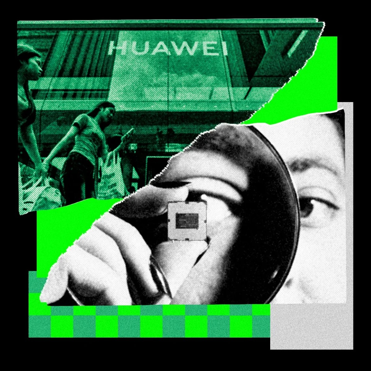
The global semiconductor landscape is witnessing a strategic pivot as Huawei Technologies, through its chip-design arm HiSilicon, signals a departure from the traditional industry roadmap defined by Moore’s Law. Tingbo He, the president of HiSilicon and a figure often referred to in domestic circles as China’s "chip queen," recently unveiled a novel architectural philosophy dubbed "Tau’s Scaling Law." This new approach aims to circumvent the physical and geopolitical barriers currently stunting China’s progress in high-end silicon production. Speaking at the IEEE International Symposium on Circuits and Systems in Shanghai, He asserted that Huawei’s engineers have identified a "new path" that prioritizes system-wide optimization over the mere miniaturization of transistors. The company’s objective is ambitious: to close the performance gap between domestic Chinese chips and Western leading-edge semiconductors within the next several years, promising a "big leap ahead" by the winter of 2026.
The Shift from Geometric Scaling to System Optimization
For decades, the semiconductor industry has been governed by Moore’s Law, the observation by Intel co-founder Gordon Moore that the number of transistors on a microchip doubles approximately every two years. This "geometric scaling" has been the primary driver of computing power, leading to the current frontier of 3-nanometer (nm) and 2-nanometer processes. However, as transistors approach the size of a few atoms, the industry is encountering the "red brick wall" of physics, where quantum tunneling and heat dissipation make further shrinking increasingly difficult and prohibitively expensive.
Huawei’s HiSilicon has reached a similar conclusion, though driven as much by necessity as by physics. "Six years ago, geometric scaling plateaued for us," Tingbo He remarked during her keynote. This timeline coincides with the imposition of stringent US export controls in 2019, which severed Huawei’s access to the world’s most advanced foundries and lithography equipment. In response, HiSilicon is shifting its focus toward what He describes as "Tau’s Scaling Law." Rather than focusing exclusively on packing more components onto a single piece of silicon, the new methodology emphasizes speeding up computations across entire circuits and computing systems.
The core of this strategy involves a technique Huawei calls "LogicFolding." This architectural innovation is designed to reduce the physical and temporal distance required to perform key logical operations within a circuit. By optimizing how logic gates are arranged and utilized, Huawei claims it can achieve performance gains that mimic the results of more advanced manufacturing nodes without requiring the same level of lithographic precision.
Navigating the Sanctions Barrier and the SMIC Factor
The backdrop of Huawei’s technological pivot is the ongoing "chip war" between Washington and Beijing. Current US Department of Commerce regulations prohibit Huawei and its subsidiaries from utilizing the services of the Taiwan Semiconductor Manufacturing Company (TSMC), the world’s preeminent foundry. TSMC currently produces the world’s most advanced 3nm chips for clients like Apple and NVIDIA using Extreme Ultraviolet (EUV) lithography machines manufactured by the Dutch firm ASML.
Under the current sanctions regime, China is barred from importing EUV equipment, forcing domestic manufacturers like Semiconductor Manufacturing International Corporation (SMIC) to rely on older Deep Ultraviolet (DUV) machines. While SMIC has successfully utilized multi-patterning techniques to produce 7nm chips for Huawei’s Mate 60 Pro smartphone—a feat that surprised many Western analysts in 2023—this process is significantly less efficient, has lower yields, and is much more expensive than EUV-based manufacturing.
By most industry estimates, China’s domestic manufacturing capability remains roughly five to seven years behind the leading edge. Huawei’s new strategy is a direct attempt to bridge this "lithography gap" through architectural ingenuity. If Huawei can achieve 1.4nm-equivalent performance using 5nm or 7nm manufacturing processes, it would effectively neutralize the impact of export controls on its high-performance computing and AI ambitions.
Technical Innovations: Interconnects and 3D Stacking
Beyond LogicFolding, Tingbo He highlighted several other pillars of the Tau Scaling Law. A primary focus is the reduction of data movement latency. In modern artificial intelligence (AI) workloads, particularly the training of Large Language Models (LLMs), the bottleneck is often not the raw speed of the processor but the time it takes for data to move between the processor and memory, or between different chips in a cluster.
"For both AI training and inference, the win is not just in shortening compute time," He explained. "It is in shortening the time that data spends moving, between chips and inside a chip." To address this, HiSilicon is investing heavily in:
- Advanced Interconnects: Developing proprietary high-speed protocols that allow chips to communicate with one another with minimal overhead, essential for scaling AI clusters to tens of thousands of GPUs.
- 3D Chip Stacking and Hybrid Bonding: Similar to Apple’s UltraFusion architecture or AMD’s 3D V-Cache, Huawei is exploring ways to stack chiplets vertically. This allows for higher component density and shorter electrical paths without requiring a smaller lithographic node.
- Nanoscale Phenomenon Accounting: Designing circuits that proactively manage the quantum effects and electronic noise that typically plague chips as they become more complex.
By viewing the chip not as an isolated component but as part of a holistic system, Huawei believes it can produce hardware that competes with Western giants like NVIDIA and Intel on a functional level, even if the underlying transistors are physically larger.
Chronology of the Huawei Semiconductor Evolution
The journey of HiSilicon reflects the broader volatility of the global tech sector over the last decade. To understand the significance of the "Tau Scaling" announcement, one must look at the timeline of Huawei’s chip development:
- 2004: HiSilicon is established as a subsidiary of Huawei, focusing initially on ASICs for telecommunications equipment.
- 2012-2018: HiSilicon rises to global prominence with its Kirin series of mobile processors, which rivaled Qualcomm’s Snapdragon in performance and efficiency.
- May 2019: The US government places Huawei on the Entity List, restricting its access to US-origin technology and software.
- August 2020: Further restrictions block Huawei’s access to any foundry using US-made equipment (effectively all major foundries, including TSMC).
- 2021-2022: Huawei pivots toward "survival mode," focusing on R&D and diversifying into software and automotive technology while stockpiling components.
- August 2023: The launch of the Mate 60 Pro featuring the Kirin 9000s chip, manufactured by SMIC on a 7nm-class process, signals Huawei’s return to the high-end smartphone market.
- May 2024: Tingbo He announces the "Tau Scaling Law" and sets a deadline for a major breakthrough by late 2026.
- 2031 Projection: Huawei aims to achieve performance equivalence to a 1.4nm process using its domestic supply chain and architectural innovations.
Industry Reactions and Critical Analysis
The announcement has met with a mixture of intrigue and skepticism from the global semiconductor community. Lennart Heim, an independent semiconductor and AI policy analyst, suggests that Huawei’s strategy is a logical response to the physical constraints of the current era. "Huawei is increasingly relying on techniques like hybrid bonding and 3D chip stacking to improve performance," Heim noted. He observed that these techniques are becoming industry standards as Moore’s Law slows down, but for Huawei, they are a mandatory alternative to the lithographic advancements they cannot access.
However, some critics argue that architectural optimization can only go so far. While "LogicFolding" and better interconnects can improve efficiency, they do not change the fundamental power-to-performance ratio inherent in the size of the transistors. Larger transistors typically consume more power and generate more heat than smaller ones. For data centers where power consumption is a primary cost driver, "equivalence" in speed may not translate to "equivalence" in total cost of ownership if the chips require significantly more cooling and electricity.
Furthermore, the 2031 goal for 1.4nm equivalence must be viewed against the roadmap of its competitors. TSMC is expected to begin mass production of actual 1.4nm chips (known as the A14 node) as early as 2027 or 2028. If Huawei reaches that performance level only in 2031, it may still find itself in a perpetual state of "catching up," albeit with a narrower gap than before.
Broader Implications for Global Technology
The success or failure of the Tau Scaling Law will have profound implications for the geopolitical balance of power. If Huawei succeeds in creating a competitive AI ecosystem using domestic silicon, it would prove that US export controls are an insufficient tool for maintaining a permanent technological lead. This could lead to a further "decoupling" of the global tech stack, with China developing a completely independent set of standards, architectures, and software ecosystems.
Moreover, Huawei’s focus on system-level optimization mirrors a broader trend in the AI industry. As the cost of training frontier models reaches billions of dollars, the efficiency of the entire computing cluster—including the networking and memory hierarchy—becomes more important than the clock speed of a single core. In this regard, Huawei’s "system-first" approach may align well with the future needs of the AI market.
As the industry looks toward the winter of 2026, the "surprise" promised by Tingbo He will be a litmus test for China’s semiconductor resilience. Whether Tau’s Scaling Law becomes a new industry standard or remains a specialized workaround for a sanctioned firm, it represents a significant chapter in the ongoing evolution of microelectronics. For now, the "chip queen" and her team at HiSilicon are betting that the future of computing lies not in how small you can build, but in how smartly you can connect.
