

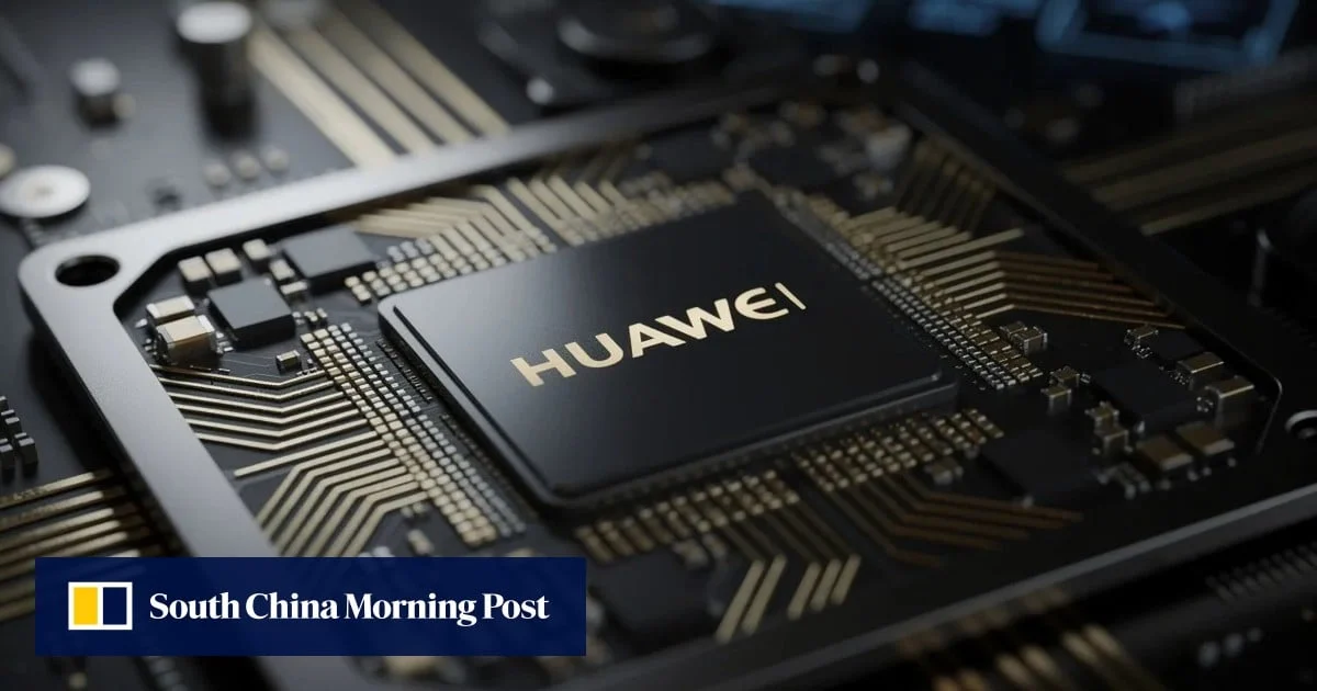
Huawei Technologies has revealed significant advancements in its semiconductor design capabilities, indicating that its upcoming Kirin 2026 mobile processor will achieve substantial performance and efficiency gains without the necessity for more advanced lithography equipment or smaller process nodes. According to new production data and a technical paper updated by the firm, the Kirin 2026 utilizes a proprietary "LogicFolding" architecture to overcome the physical limitations currently imposed by international trade restrictions and the slowing of traditional Moore’s Law scaling. The data, published on the ChinaXiv scientific preprint platform, suggests that Huawei has successfully increased transistor density by 55 per cent compared to the previous generation Kirin 9030 Pro, despite utilizing the same manufacturing process node.
This development is centered on the "Tau Scaling Law," a theoretical framework first introduced in May 2024 by He Tingbo, the chairwoman of the Huawei Scientist Committee and president of HiSilicon, Huawei’s internal semiconductor design arm. Known in the industry as the "chip queen," He Tingbo has spearheaded Huawei’s efforts to maintain competitiveness in the high-end smartphone market following the imposition of US export controls that have blocked the company’s access to advanced Extreme Ultraviolet (EUV) lithography tools. The new data provides the first concrete engineering evidence that Huawei’s architectural innovations are yielding measurable improvements in transistor distribution and power management.
The Evolution of the Tau Scaling Law and LogicFolding Architecture
The semiconductor industry has traditionally relied on geometric scaling—the process of physically shrinking transistors to fit more of them onto a single silicon die. This path, however, has become increasingly difficult and expensive as physical limits are reached and as geopolitical barriers prevent certain firms from accessing the latest 3-nanometer and 2-nanometer fabrication technologies. Huawei’s Tau Scaling Law proposes an alternative path, focusing on the topological reorganization of logic rather than mere physical miniaturization.
The LogicFolding architecture is the practical application of this law. By utilizing a double-layer folding structure, Huawei has fundamentally altered the spatial distribution of logic gates on the chip. This approach allows for a "topological reorganization" that maximizes the utility of existing process nodes. According to the updated research paper, the gains achieved in the Kirin 2026 would have traditionally required three years of standard geometric scaling and a transition to a more advanced lithography step. Instead, Huawei has achieved these results through design-level innovation, effectively decoupling performance growth from the immediate need for next-generation fabrication hardware.
Technical Specifications and Performance Metrics
The production data released by Huawei provides a detailed look at the efficiency and density gains of the Kirin 2026. Operating at a standard 25 degrees Celsius with a voltage of 0.9V, the processor demonstrated a 41 per cent reduction in power consumption compared to the Kirin 9030 Pro baseline while maintaining the same level of performance. This is a critical metric for mobile devices, where thermal management and battery life are primary concerns for flagship handsets.
Furthermore, the Kirin 2026 achieved a 5.6 per cent decrease in power density. This suggests that the LogicFolding architecture not only makes the chip more efficient but also helps in spreading the heat generated across the die more effectively, reducing the risk of thermal throttling during intensive tasks such as gaming or artificial intelligence processing.
The architectural shift has also led to significant improvements in signal integrity and latency. The report highlights three key engineering achievements:
- Wire Length Reduction: The double-layer folding architecture has shortened the distance signals must travel by 30 per cent. Shorter wires result in lower resistance and capacitance, which directly contributes to higher speeds and lower power loss.
- Clock-Buffer Optimization: The count of clock buffers—components used to synchronize the timing of signals across the chip—has been reduced by over 50 per cent. This reduction simplifies the chip’s internal circuitry and saves significant die area.
- Clock Skew Improvement: Clock skew, the phenomenon where the clock signal arrives at different components at different times, has been reduced by 25 per cent. Improving synchronization allows the processor to operate at higher frequencies with greater stability.
Chronology of Huawei’s Semiconductor Resilience
The development of the Kirin 2026 and the Tau Scaling Law is the latest chapter in a multi-year effort by Huawei to rebuild its semiconductor pipeline in the face of external pressures.
- May 2019: The US Department of Commerce placed Huawei on the Entity List, restricting its access to US-origin technology, including advanced EDA (Electronic Design Automation) software and foundry services from TSMC.
- 2020–2022: Huawei’s Kirin chip production was largely halted, forcing the company to rely on stockpiled chips and 4G-only versions of Qualcomm processors for its flagship devices. During this period, HiSilicon shifted its focus toward research and development of domestic alternatives and architectural breakthroughs.
- August 2023: Huawei surprised the global market with the launch of the Mate 60 Pro, featuring the Kirin 9000S. This chip, manufactured by China’s SMIC using a 7-nanometer-class process, proved that Huawei could still produce 5G-capable silicon despite sanctions.
- May 2024: He Tingbo officially introduced the Tau Scaling Law at a technical forum, outlining the theoretical basis for increasing chip performance through architectural folding and topological optimization.
- September 2024: Updated research and production data for the Kirin 2026 were published on ChinaXiv, confirming the practical success of the LogicFolding architecture in the upcoming flagship series.
Domestic Context and the Role of HiSilicon
The success of the Kirin 2026 is a testament to the strategic pivot led by He Tingbo. As the president of HiSilicon, she has transitioned the department from a design house that optimized ARM-based designs for TSMC’s leading-edge nodes to an innovation hub focused on fundamental semiconductor physics and architecture. The "Chip Queen’s" strategy emphasizes "vertical integration" and "architectural sovereignty," aiming to ensure that Huawei’s product roadmap is no longer entirely dependent on the global lithography roadmap controlled by ASML and its peers.
Industry analysts in China have noted that this approach aligns with the broader national goal of "Self-Reliance and Self-Improvement in Science and Technology." By maximizing the potential of DUV (Deep Ultraviolet) lithography—which is still accessible to Chinese foundries—through advanced design techniques like LogicFolding, Huawei is providing a blueprint for other domestic firms facing similar technological constraints.
Market Implications and Competitive Landscape
The Kirin 2026 is slated to power Huawei’s next generation of Mate flagship smartphones, traditionally launched in the autumn. The 55 per cent increase in transistor density suggests that Huawei intends to narrow the performance gap with rivals like Apple’s A-series and Qualcomm’s Snapdragon chips, which currently benefit from TSMC’s 3-nanometer processes.
If Huawei can deliver a flagship experience that rivals the iPhone 16 or upcoming Snapdragon 8 Gen 4 devices using older manufacturing nodes, it could significantly shift market dynamics in China and other regions where Huawei remains a major player. The ability to achieve high performance with lower power consumption is particularly vital as mobile AI (Artificial Intelligence) becomes a standard feature, requiring sustained processing power without excessive heat generation.
However, the industry remains cautious. While the data from ChinaXiv is promising, the paper has yet to undergo full peer review, and the real-world performance of the Kirin 2026 will only be confirmed once the devices hit the consumer market. Competitors are also not standing still; Apple and Qualcomm are moving toward more advanced packaging techniques and N3E/N3P nodes, which offer their own sets of efficiency gains.
Geopolitical and Global Industry Impact
The announcement of the Tau Scaling Law’s success serves as a signal to the global semiconductor community that the "node-centric" view of progress is being challenged. For decades, the industry has measured progress by the "nanometer" label. Huawei’s move toward "architectural scaling" suggests that the design phase of chipmaking may become just as critical as the fabrication phase in determining a device’s ultimate capabilities.
From a geopolitical perspective, this development suggests that US-led export controls may have the unintended consequence of accelerating Chinese innovation in alternative semiconductor pathways. By being forced to innovate within the constraints of existing lithography, Huawei is exploring "More than Moore" strategies—such as 3D IC, advanced packaging, and now LogicFolding—that the rest of the industry might not have prioritized as aggressively while the path to 2nm remained clear.
Conclusion and Future Outlook
The Kirin 2026 represents a pivotal moment for Huawei and the broader Chinese semiconductor industry. By achieving a 55 per cent density boost and a 41 per cent power reduction through the LogicFolding architecture, Huawei is demonstrating that architectural innovation can compensate for a lack of access to the world’s most advanced manufacturing tools.
As the firm prepares for the autumn launch of its latest flagship handsets, the focus will shift from theoretical papers to consumer performance. If the Kirin 2026 delivers on the promises of the Tau Scaling Law, it will validate He Tingbo’s vision of a new era of semiconductor design—one where the arrangement of logic is just as important as the size of the transistor. For the global market, it serves as a reminder that technological progress is rarely a linear path and that constraints often breed the most significant breakthroughs.
